
Hello, friends!
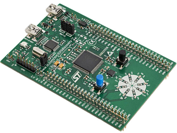
STM32F3 Discovery board is a great device for studying robotics and mobile automotive tools. It contains fast MCU Cortex-M4 @ 72MHz, 40+8 kB RAM, 256 kB Flash, dozens of I/O ports for peripheral units, built-in gyroscope and accelerometer, on-board ST-LINK/V2 for programming and debugging. This board is good enough to develop a flight-controller or a fancy smart robot.
This guide describes how to get started programming SMT32F3 board using IAR Embedded Workbench.
Understanding Led Blinking
Now we will create and explain a simple LED blinking firmware for the STM32F3 Discovery board. This evaluation board has several LEDs. In the “User manual (UM1570)” you can find MCU pin description and port connection schema in Table 6 on page 28.
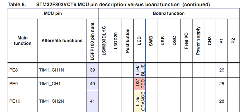
We will use port E pin 8 for blue LED blinking. It seems to be an ordinary task. In fact it includes some complex routines that are not visible at the first sight. After reset the device is running from HSI (8 MHz) and all peripherals are off except internal SRAM, Flash and SWD. The clock for all peripherals is switched off, except the SRAM and FLASH.
You might know that every program starts at main() function. In fact before the main() function is called the start up code initializes MCU, interrupt table and configures crystal oscillator. For example, the “SetSysClock()” function in system_stm32f30x.c file configures MCU @ 72 MHz (HSE 8MHz x 8 PLL).
  #include <stm32f30x.h>
  #include <stm32f30x_rcc.h>
  #include <stm32f30x_gpio.h>

  #define LED    GPIO_Pin_8

  int main()
  {
        long i;
        GPIO_InitTypeDef gpio;

        // Blue LED is connected to port E, pin 8 (AHB bus)
        RCC_AHBPeriphClockCmd( RCC_AHBPeriph_GPIOE, ENABLE );

        // Configure port E (LED)
        GPIO_StructInit( &gpio );
        gpio.GPIO_Mode = GPIO_Mode_OUT;
        gpio.GPIO_Pin  = LED;
        GPIO_Init( GPIOE, &gpio );

        // Blinking LEDS
        while(1)
        {
                // On
                GPIO_SetBits( GPIOE, LED );
                for( i = 0; i < 500000; i++ );
                // All off
                GPIO_ResetBits( GPIOE, LED );
                for( i = 0; i < 500000; i++ );
        }
  }
We use the SPL (Standard Peripheral Library) in our development process.
- 1) Include header files from the SPL library for our firmware: stm32f30x.h – main header file with data types, constants and structures; stm32f30x_rcc.h – the reset and clock control data types, constants and functions; stm32f30x_gpio.h – required stuff for general-purpose i/o (GPIO) ports initialization, configuration, read/write.
- 2) Call the “RCC_AHBPeriphClockCmd()” function to enable GPIO port E located on AHB (Advanced High-performance Bus). Most peripheral units are turned off by default that is why we must enable and sometimes setup its clock prescaler. We will talk about buses a little bit later.
- 3) Declare the GPIO_InitTypeDef data structure variable named “gpio” and initialize it with the default values by call to the GPIO_StructInit(&gpio) function. Fill the structure fields with our values – “mode” is set to output and “pin” number is assigned 8. Finally the port E is activated by call to the GPIO_Init() function.
- 4) In the endless ‘while(1)’ loop Pin_8 is switched on and off thus making LED blink. To slow down blinking we use delays “for( i = 0; i < 500000; i++ );".
The source code can be compiled, linked and the firmware is ready to be downloaded into the STM32F3 board.
STM32 Bus Architecture
In the led blinking firmware we enabled clocking of the GPIO (general-purpose I/O) port and its bus. STM32F3 is an ARM Cortex-M4 microcontroller that contains many functional blocks. These blocks are connected to the standard Advanced Microcontroller Bus Architecture (AMBA). This multi-layered 32-bit bus is composed of several masters and slaves. Besides, there are two AHB (Advanced High-performance Bus) to APB (Advanced Peripheral Bus) bridges. The data flow looks like: CPU → AHB → APB → GPIO.
MCU core controls the data flow over the buses and firmware developer does not need to know its internals. But it is important to understand how to configure peripheral devices connected to this bus.
I should mention that APB1 is a slow bus. Its speed is limited to 36MHz. Every peripheral device connected to APB1 (for example SPI2) will work slower than similar peripheral unit connected to APB2 (for example, SPI1). APB2 bus operates at maximum MCU clock speed @ 72MHz.
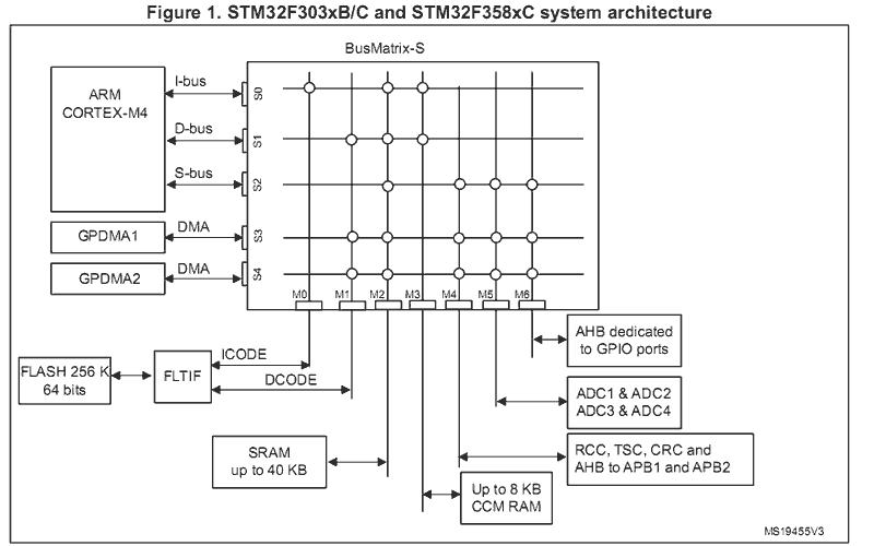
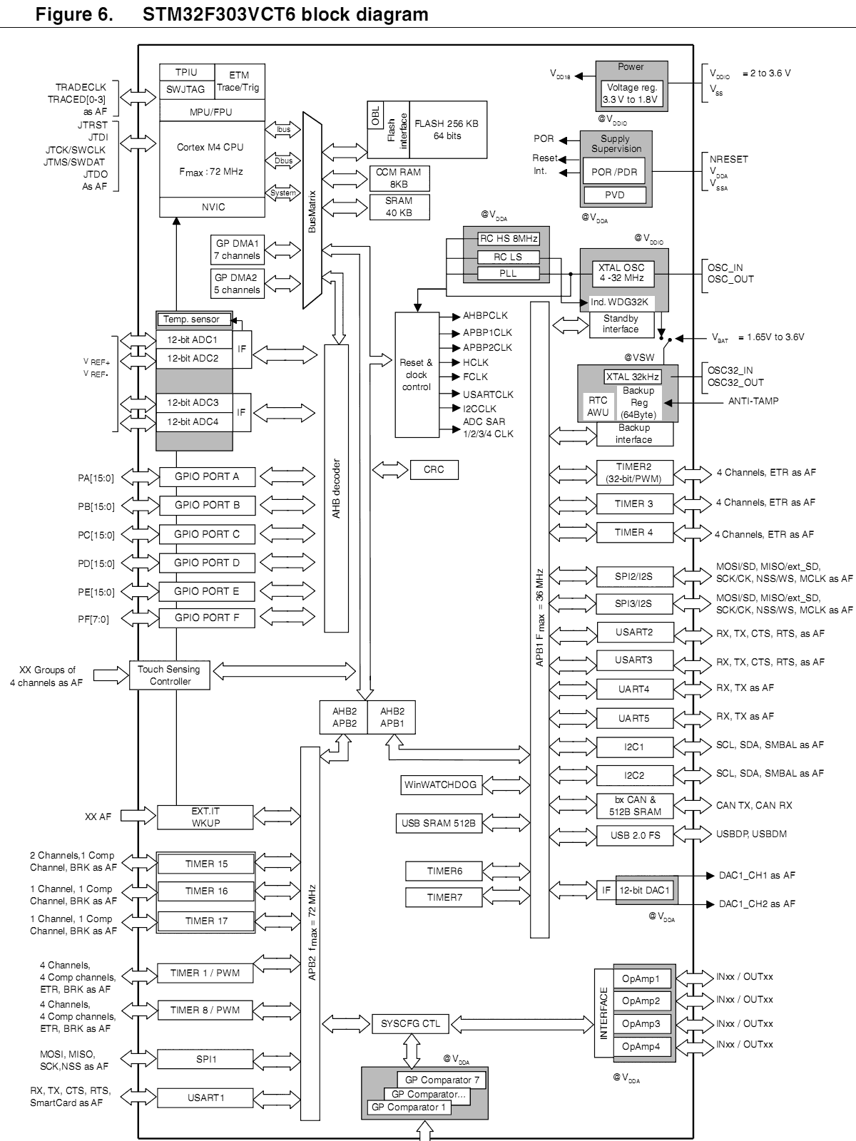
BusMatrix is a sort of multiplexer used to route data flow between MCU/Memory and peripheral units. The STM32 Bus Matrix diagram can be found on page 49 of the SMT32F3 Reference Manual. This picture gives an understanding of how the bus multiplexer is designed. In the User Manual I have found great block diagram of the STM32F303VCT6 MCU. Every peripheral block such as GPIO, RCC, SPI, ADC, Timers, etc, can be located in the picture.
There is another interesting feature in the STM32 MCU called peripheral interconnect matrix. Some peripheral units can work autonomous with each other. Usually it is a pair, such as Timer and some I/O unit, for example DMA or ADC. The text version of the peripherals interconnect matrix can be found in Table 22 of the Reference Manual (page 112, Ch.8). Knowing these interconnections allows the following benefits:
- Autonomous and fast communication between peripherals,
- Efficient synchronization between peripherals,
- Optimize number of available pins in any packages.
Interconnection details are described in different sections of the Reference Manual. I think we should keep in mind this feature and use it when possible to improve performance.
GPIO Structure and Configuration
Processors in the STM32 family have very flexible and at the same time very powerful general purpose input-output (GPIO) ports hardware. Although the STM32 is a 3.3V MCU some its port pins are 5V tolerant and compatible with many I/O shields. Every port contains 16 pins (0-15). Port pins can be individually configured. Port pin can operate in one of four modes: digital input, digital output, alternate (for example SPI CLK), analog i/o.
I should say a few words about Alternate function (AF). It means that a port pin is controlled by a hardware peripheral module, for example SPI, I2C, UART. A pin can behave as a clock line or a data line for specific communication protocol. In the User manual you can find table #6 where all functions are listed. The MCU multiplexer allows only one peripheral alternate function (AF) connected to an I/O pin at a time.
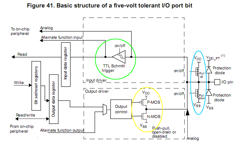
The hardware basic structure of a port pin is shown in the figure. There are three important built-in units:
- pull-up and pull-down resistors;
- Schmitt trigger helps to avoid input signal and contact bouncing;
- p-mos and n-mos transistors manage pin state in push-pull mode and in open-drain mode.
In the table below I have collected typical configuration settings for GPIO port pins.
| Peripheral | Configuration | Mode | Pull | Comment |
|---|---|---|---|---|
| LED | OUT, 2MHz | PP | Up, Down | Pull-Up and Pull-Down are often used; See schematics |
| BUTTON | IN, 2MHz | – | Pull-Down | Usually buttons are connected to the GND through resistor; 2MHz slow speed will filter contact bouncing |
| ADC | In, Analog | – | NoPull | Select proper speed |
| USART | AF, 50MHz | PP | Pull-Up | Sometimes pull-down circuit is used |
| SPI | AF, 50MHz | PP | Pull-Up | Speed is important |
| I2C | AF, 50MHz | Open Drain | NoPull | Open Drain mode, pull-up resistors are always required |
| USB | AF, 50MHz | PP | NoPull | Typical configuration, 48MHz |
| CAN | AF9, 2MHz | PP | NoPull | Slow speed will filter signal |
For example, a typical hardware I2C connection between the host master and the slave target requires pull-up resistors. The master and the target are connected together via the data (SDA) and clock (SCL) pins. A 4.7 kOhm pull-up resistor has to be connected to both the SDA and SCL lines. GPIO port pins for I2C interface in the STM32 example are configured as GPIO_PuPd_NOPULL. I think the reason for this is that there are two pull-up resistors already connected to VCC. There is no need to activate built-in resistors.
Most popular and universal pin mode is Push-Pull (PP). It is the default setting in the GPIO_StructInit() function. Besides, by default the pull-up and pull-down resistors (~1kOhm) are not used and the corresponding default value is GPIO_PuPd_NOPULL. Pull-up and Pull-down resistors can be used to ensure that the signal will be a valid logic level if external devices are disconnected.
In open-drain (GPIO_OType_OD) mode: A “0” in the Output register activates the N-MOS, whereas a “1” in the Output register leaves the port in Hi-Z (the P-MOS is never activated).
In Push-pull (GPIO_OType_PP) mode: A “0” in the Output register activates the N-MOS, whereas a “1” in the Output register activates the P-MOS.
Keep in mind that STM32 MCU operates at 3.3V. Luckily many GPIO port pins are 5V tolerant (FT – five volt tolerant). I recommend to take a look at STM32F303 Datasheet if you plan to connect 5V devices. In the table 13 you will find characteristics for different packages (LQFP100, 64, 48) and its pins features (FT, I/O, AF).
I am happy to inform you that maximum “Output Current Sunk by any I/O and Control Pin, mA” is equal to 25mA. Unfortunately, “Total output current sunk by sum of all IOs and control pins” is limited to 80 mA.
Now we are ready to write a simple firmware that demonstrates the I/O techniques. The BUTTON is used as an input device and the LEDS are used as a simple output device. When the BUTTON is pressed we light on the LEDS, otherwise the LEDS are turned off.
#include <stm32f30x.h>

#define LEDS    (GPIO_Pin_8 | GPIO_Pin_9 | GPIO_Pin_10 | GPIO_Pin_11)
#define BUTTON  GPIO_Pin_0

int main()
{
	GPIO_InitTypeDef gpio;

	RCC_AHBPeriphClockCmd( RCC_AHBPeriph_GPIOA, ENABLE );
	RCC_AHBPeriphClockCmd( RCC_AHBPeriph_GPIOE, ENABLE );

	//---------------------------------------------------//
	// Port A - pushbutton
	GPIO_StructInit( &gpio );
	gpio.GPIO_Mode = GPIO_Mode_IN;
	gpio.GPIO_Pin  = BUTTON;
	GPIO_Init( GPIOA, &gpio );

	//---------------------------------------------------//
	// Port E - LEDS
	GPIO_StructInit( &gpio );
	gpio.GPIO_Mode = GPIO_Mode_OUT;
	gpio.GPIO_Pin  = LEDS;
	GPIO_Init( GPIOE, &gpio );

	//---------------------------------------------------//
	while(1)
	{
		// The Schmitt trigger filters input signal.
		// We have no problems with contact bouncing.
		//------------------------------------------
		// Polling pushbutton state
		if( GPIO_ReadInputDataBit(GPIOA, BUTTON) )
		{
			GPIO_SetBits( GPIOE, LEDS );
		}
		else
		{
			GPIO_ResetBits( GPIOE, LEDS );
		}
	}
}
Hope this article will help to understand the internals of the GPIO architecture. It can be used as a quick guide to STM32F303. Feel free to leave any comments. Good luck!